

Provide you with enterprise-level interconnection chips
Severity: Notice
Message: Undefined index: title
Filename: views/single_product.php
Line Number: 17
Backtrace:
File: /data/user/htdocs/en/app/views/single_product.php
Line: 17
Function: _error_handler
File: /data/user/htdocs/en/app/controllers/Category.php
Line: 516
Function: view
File: /data/user/htdocs/en/index.php
Line: 317
Function: require_once

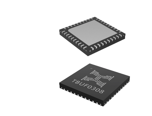
8-output differential clock buffers with super-low additional jitter
Single-end, differential, and crystal inputs are flexibly supporte
8 differential outputs, with the maximum frequency up to 1.5GHz; LVPECL, LVDS, and HCSL modes are supported
Additional jitter<30fs (@100MHz HCSL mode)
Compatible with PCIe1.0~5.0 clock specifications
Operating temperature: -40°C~85°C
Package: QFN40
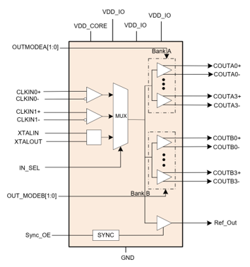
TBUF0308 is a high-performance clock buffer. It supports 8 channels of 1.5GHz differential super low jitter outputs, which are mainly used for low jitter, high-frequency clocking and level shifting, and so on. The buffer supports 3 modes of clock source inputs, such as single-end clock, differential clock, or crystal. TBUF0308 can be assigned to two output groups, group A and group B, and one LVCMOS output. The outputs in groups A and B can be independently configured to LVPECL, LVDS, HCSL or HIZ mode. The LVCMOS clock output can be enabled or disabled in sync with the selected clock. TBUF0308 supports a flexible voltage range, with both core and IO voltages supporting either 2.5V or 3.3V.

Application Diagram


Server


Storage


Switch


Router
Copyright ? 2000-2023 成都電科星拓科技有限公司 版權(quán)所有 備案編號(hào): 蜀ICP備2022009451號(hào) 川公網(wǎng)安備 51019002004893號(hào)